ETROYL Academy · FPGA & Digital Design · VHDL Engineering
SuperUART: Beyond Fixed Baud Rates — Automatic Baud-Rate Detection for FPGA-Based UART Communication
An FPGA-oriented UART implementation that measures the master’s bit timing from a known initialization pattern instead of requiring a predefined baud-rate selection.
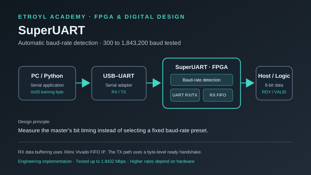
The project README reports successful testing from 300 baud to 1,843,200 baud (1.8432 Mbps). Higher rates are a hardware-dependent design possibility, not a performance result claimed by that test record.
01 · Motivation
What if UART did not need a fixed baud-rate preset?
Many UART implementations select from a set of conventional baud rates and derive a local bit period using a clock divider, often combined with oversampling. SuperUART explores a different approach for FPGA-based links: measure a known training pattern from the master, then use the measured timing to establish the UART timing reference.
The aim is not to add one more standard rate to a menu. It is to make the communication block adapt to the timing of the transmitting endpoint, within the limits of the FPGA clock and physical implementation.
02 · Core mechanism
Using 0x55 to detect the master’s bit timing
When SuperUART is in its initial state, the master sends the byte 0x55 as an initialization pattern. Its alternating bits create repeated signal transitions, giving the detection logic timing edges to measure.
0x55 pattern from the master.The RTL contains baud-detection logic that measures transition intervals and establishes a timing period, including a half-period reference used by the UART timing generator. This is different from simply choosing a conventional baud-rate constant or relying on a fixed 16× oversampling clock.
0x76B19D08; source-code users can change or disable this feature.03 · FPGA architecture
UART logic, buffering and integration
SuperUART is implemented in VHDL and includes the baud-rate detection logic, an 8-bit UART receiver and transmitter, a receive FIFO and a byte-level transmit handshake. A wrapper is provided to make the core easier to integrate into a larger FPGA design.
Before looking at individual ports, it helps to distinguish three views: the packaged IP interface, its configuration GUI, and a complete example design. They show different levels of the same system rather than three separate UART implementations.

Transmit and RDY2Transmit form a byte-level control handshake; they are not the serial TX wire itself.
0x55 initialization byte rather than selected from a fixed baud-rate menu.In the simple design below, received data is used directly by the example logic. This makes it easier to understand the UART interface before moving to the more complex UART-to-I²C application.

RDY2Transmit to go high, place the byte on TX_DATA, and raise Transmit from low to high. Keep TX_DATA stable and hold Transmit high until RDY2Transmit goes low; then lower Transmit. The serial frame starts on the next internal bit-clock boundary, so it may begin up to one bit time after the request.- RX FIFO: uses Xilinx Vivado FIFO IP backed by FPGA memory resources, with depth configurable within the selected device and IP configuration limits.
- TX interface: accepts a byte through
TX_DATAwhenRDY2Transmitis high; theTransmitinput is triggered by a rising edge. The documented design does not include a TX FIFO. - RX interface: received bytes are buffered and read through
RX_DATAandRead_RX.RX_Data_Validindicates when the read data is valid. - Status: FIFO full/empty and write acknowledgement signals help the surrounding logic manage data flow.
- Reset: provides active-low hardware reset and optional software-triggered reinitialization.
Key interface signals
| Signal | Direction / role | Usage |
|---|---|---|
CLK | Input | Main FPGA clock. The documented requirement is at least four times the desired baud rate. |
rst_n | Input | Active-low hardware reset. |
RX / TX | Serial input / output | Connect to the other endpoint’s TX / RX respectively; ensure the RX line is pulled high when idle. |
TX_DATA | 8-bit input | Byte to transmit. |
Transmit | Control input | Rising-edge request to transmit a byte when RDY2Transmit is high. |
RDY2Transmit | Status output | High when the transmitter can accept a new byte; low while transmitting. |
RX_DATA | 8-bit output | Data read from the receive FIFO. |
Read_RX | Control input | Rising-edge request to read received data from the FIFO. |
RX_Data_Valid | Status output | Indicates that the requested RX data is valid. |
BUFF_EMPTY / BUFF_FULL | Status outputs | Indicate receive FIFO availability and full condition. |
fifo_wr_ack | Status output | Indicates that the received data has been written into the FIFO. |
The documented interface uses 8-bit data without parity checking. Consult the RTL and Vivado IP configuration for the exact integration details of a particular build.
04 · Operating range
Measured results and hardware-dependent limits
| Successfully tested minimum | 300 baud |
|---|---|
| Successfully tested maximum | 1,843,200 baud (1.8432 Mbps), the maximum PC-generated rate reported in the README |
| Documented clock relationship | Main clock frequency must be at least 4× the desired baud rate |
| Illustrative theoretical ceiling | At a 100 MHz main clock, 25 Mbps follows from the 4× relationship, provided the FPGA implementation and hardware support it |
The 25 Mbps figure is a design-bound example, not a claim that this rate has been validated. Practical performance depends on clocking, timing closure, FPGA I/O, the external interface and signal integrity. The reported test range is the evidence-backed result.
05 · Application case study
From a Python script to an Si570 clock generator
SuperUART was also used in a practical FPGA control path. A Python program on a PC sends commands over a serial connection. FPGA logic decodes the commands and uses an I²C master to read or write registers of an Si570 clock generator, returning read data over UART.

Command patterns in the example
A0 B0 C0 D0identifies an I²C read command, followed by the slave-address and register-address bytes.A5 B5 C5 D5identifies an I²C write command, followed by the slave-address, register-address and data bytes.76 B1 9D 08is the default software-reset key when that feature is enabled.
This case study demonstrates how a serial IP block can be integrated into a larger FPGA application; the bridge and I²C master are application-specific components rather than part of the core UART’s baud-detection mechanism.
06 · Scope and limitations
An engineering resource, not a hardened PHY claim
SuperUART is shared to make its design approach and implementation available for study. It should not be interpreted as a fully hardened communications PHY or as a guarantee of operation at every possible baud rate.
- Baud-rate detection depends on the known initialization pattern being received well enough for its timing to be measured.
- The design does not implement sophisticated rejection of noise or deformed training data.
- High-speed operation must be validated in the target FPGA, with its actual clock constraints, I/O configuration, board and interconnect.
- The receive side uses FIFO buffering; the documented transmit side uses a ready/handshake interface rather than a TX FIFO.
These boundaries are part of the engineering context and should be considered when adapting the design to a new system.
07 · Explore the source
Study the VHDL and example integration
The repository includes the VHDL source, Vivado IP integration files, a testbench and a Python example for the UART-to-I²C Si570 application. Reviewing the source alongside the README is the recommended starting point for understanding the implementation and adapting it to a target design.
Open the project repository to inspect the implementation and supporting files.
Explore the SuperUART repository →Questions about this resource or a possible engineering application? Contact ETROYL.